
 By Adri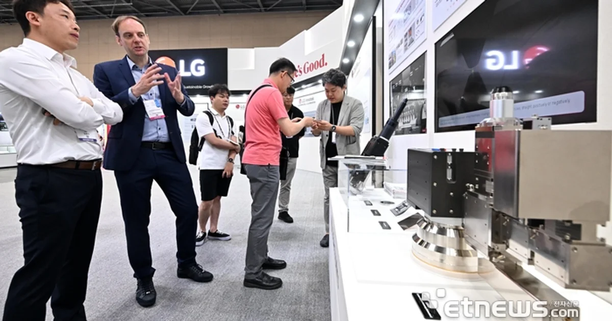
LG gets its first industrial LDI customer
LG Electronics has secured its first commercial order for a Laser Direct Imaging, or LDI, system designed for semiconductor packaging.
The contract was signed by LG Electronics' Production Engineering Research Institute with a global OSAT provider. These companies specialize in assembling, packaging and testing chips after semiconductor fabrication.
The customer's identity has not been disclosed. Korean reports only describe it as a global OSAT company that also operates packaging facilities in South Korea.
That distinction matters. LG had previously supplied a system for university research, but this is its first order for equipment intended for an industrial mass-production line.
No mask: the laser draws the circuit directly
LDI works differently from conventional lithography based around a physical photomask.
The required pattern exists as digital data and a laser directly exposes the appropriate areas of the substrate.
A dedicated physical mask therefore does not need to be manufactured for every pattern.
That can reduce some costs, shorten production changes and provide greater flexibility when the circuit layout needs to be adjusted.
LG reaches 1.5 micrometers
LG currently has several versions of the equipment offering resolutions of 1.5, 3 and 5 micrometers.
Its highest-resolution model can produce line-and-space patterns around 1.5 micrometers and uses a 405 nm laser-diode light source.
The system can also process substrates as large as 600 x 600 mm, which is particularly relevant as panel-level packaging develops.
At these dimensions, the machine is not patterning the transistors themselves. LDI operates later in manufacturing to form fine electrical interconnects used inside semiconductor packages.
The real advantage appears when the substrate is no longer perfectly flat
Advanced packaging creates a problem that marketing diagrams rarely show: materials move.
Heat, manufacturing processes and mechanical stresses can cause large substrates to expand, contract or warp slightly.
With a fixed photomask, the circuit geometry remains where the mask says it should be. If the substrate has shifted by a few micrometers, accurate alignment becomes significantly more difficult.
LG's system can instead measure positions and shapes before exposure and digitally compensate the pattern sent to the laser.
LG promotes this capability as a way to improve yield when extremely fine interconnects need to be produced on substrates that may have changed shape.
Why AI suddenly makes this market so valuable
The timing is obviously not accidental.
Modern AI accelerators increasingly combine multiple components in one system: compute dies, HBM stacks, extremely high-speed interconnects and sometimes specialized chiplets.
Packaging can therefore no longer be treated as little more than the enclosure around a finished chip.
A growing share of system performance depends directly on the density and quality of the connections between these components.
Technologies such as TSMC's CoWoS and Intel's EMIB illustrate the growing importance of advanced packaging.
But LG has not won a CoWoS contract from TSMC
That is an important distinction.
TSMC's packaging capacity is under intense pressure from AI-accelerator demand, and CoWoS is frequently described as one of the industry's major capacity constraints.
That makes advanced-packaging equipment attractive to a growing number of suppliers.
However, nothing in LG's current order establishes that its machine will be used by TSMC or directly inside a CoWoS production line.
The customer is an unnamed OSAT company. CoWoS is therefore part of the broader industrial context, not the contract itself.
LG is entering a market with established specialists
LG did not invent Laser Direct Imaging and it is not entering an empty market.
Existing suppliers include companies such as SCREEN Holdings, ORC Manufacturing and other international manufacturers of direct-imaging equipment.
LG does have an unusual advantage: it has spent decades developing production technologies for companies inside its own industrial group.
Its production engineering institute dates back to 1987 and previously commercialized LDI equipment for display manufacturing before adapting the technology for semiconductor packaging.
The progression is fairly logical. A technology already used for displays has gradually been pushed toward the dimensions required for advanced-package interconnects.
More semiconductor machines are already coming
LG does not appear to view LDI as a one-off product.
The company is also developing inspection systems for HBM and laser equipment for creating Through-Glass Vias in future glass substrates.
TGVs are vertical electrical connections passing through glass. They are among the technologies being explored for larger, denser packages containing more interconnected chips.
LG has also demonstrated laser drilling, bonding, redistribution-layer formation and inspection equipment.
Packaging is becoming a strategic industry of its own
For years, the semiconductor industry's most visible announcements revolved around process nodes: 7 nm, 5 nm, 3 nm and now 2 nm.
That race continues, but gaining more performance is no longer simply a matter of shrinking transistors.
Correctly assembling multiple dies, bringing memory closer to compute and maintaining thousands of fast interconnects is becoming almost equally important.
That is exactly why more companies want to sell the equipment needed for those manufacturing steps.
LG's first order looks small next to the billions being invested by TSMC, Samsung or Intel. But it points to something much larger: the AI-chip race is no longer fought only inside semiconductor fabs. It is increasingly fought in the machines responsible for connecting everything that comes out of them.